QSFP-100G-LR4, PEAK QSFP28 100GBASE-LR4 4x1310 Duplex LC 10km DDM
Features
- Hot pluggable QSFP28 MSA form factor
- Compliant to IEEE 802.3ba 100GBASE-LR4
- Supports 103.1Gb/s aggregate bit rate
- Up to 10km reach for G.652 SMF
- Single +3.3V power supply
- Operating case temperature: 0~70oC
- Transmitter: cooled 4x25Gb/s LAN WDM DFB TOSA (1295.56, 1300.05, 1304.58, 1309.14nm)
- Receiver: 4x25Gb/s PIN ROSA
- 4x25G electrical interface (OIF CEI-28G-VSR)
- Maximum power consumption 3.5W
- Duplex LC receptacle
- RoHS-6 compliant
Applications
- 100GBASE-LR4 Ethernet Links
- Infiniband QDR DDR and EDR interconnects
- Client-side 100G Telecom connections
The QSFP-100G-LR4 is a transceiver module capable of transmitting at 100Gb/s, designed specifically for optical communication applications compliant with the IEEE 802.3ba standard 100GBASE-LR4. The module utilizes 4 input channels of 25Gb/s electrical data, converting them into 4 channels of LAN WDM optical signals, which are then multiplexed into a single channel for 100Gb/s optical transmission. Conversely, on the receiver side, the module de-multiplexes a 100Gb/s optical input into 4 channels of LAN WDM optical signals and then converts them to 4 output channels of electrical data.
The LAN WDM channels have central wavelengths of 1295.56, 1300.05, 1304.58, and 1309.14 nm, which are part of the LAN WDM wavelength grid defined in IEEE 802.3ba. The module features high-performance cooled LAN WDM DFB transmitters and high-sensitivity PIN receivers, ensuring superior performance for 100Gigabit Ethernet applications up to 4km links, while also meeting the optical interface requirements specified in IEEE 802.3ba Clause 88.
The QSFP-100G-LR4 module conforms to the QSFP+ Multi-Source Agreement (MSA) in terms of form factor, optical/electrical connection, and digital diagnostic interface. It has been designed to operate effectively under the harshest external conditions, including temperature, humidity, and EMI interference.
The QSFP-100G-LR4 module receives 4 channels of 25Gb/s electrical data, which are processed by a 4-channel Clock and Data Recovery (CDR) IC that reshapes and reduces the jitter of each electrical signal. The DFB laser driver IC converts each of the 4 channels of electrical signals to an optical signal transmitted by one of the 4 cooled DFB lasers in the Transmitter Optical Sub-Assembly (TOSA), with each laser launching the optical signal at a specific wavelength specified in IEEE 802.3ba 100GBASE-LR4 requirements. The 4-lane optical signals are then optically multiplexed into a single fiber by a 4-to-1 optical WDM MUX. An automatic power control (APC) circuit maintains the optical output power of each channel constant, and the transmitter output can be turned off using the TX_DIS hardware signal and/or 2-wire serial interface.
On the receiver side, the module receives 4-lane LAN WDM optical signals, which are de-multiplexed by a 1-to-4 optical DEMUX. Each resulting channel of optical signals is fed into one of the 4 receivers in the Receiver Optical Sub-Assembly (ROSA), which converts the optical signal to an electrical signal. The regenerated electrical signals are retimed, de-jittered, and amplified by the RX portion of the 4-channel CDR, and the retimed 4-lane output electrical signals are compliant with IEEE CAUI-4 interface requirements. The DOM section monitors each received optical signal, and the monitored value is reported through the 2-wire serial interface. If any received optical signal is weaker than the threshold level, the RX_LOS hardware alarm will be triggered.
The module requires a single +3.3V power supply, with both power supply pins VccTx and VccRx internally connected and applied concurrently. It features 7 low-speed hardware control pins, including the 2-wire serial interface (ModSelL, SCL, SDA, ResetL, LPMode, ModPrsL, and IntL). ModSelL is an input pin that allows the use of the product on a single 2-wire interface bus, and SCL and SDA are required for 2-wire serial bus communication interface. The ResetL pin enables a complete reset, and the LPMode pin sets the maximum power consumption for the product. The ModPrsL signal indicates module presence, and the IntL pin is an output pin that indicates possible operational faults or statuses critical to the host system, identified using the 2-wire serial interface.
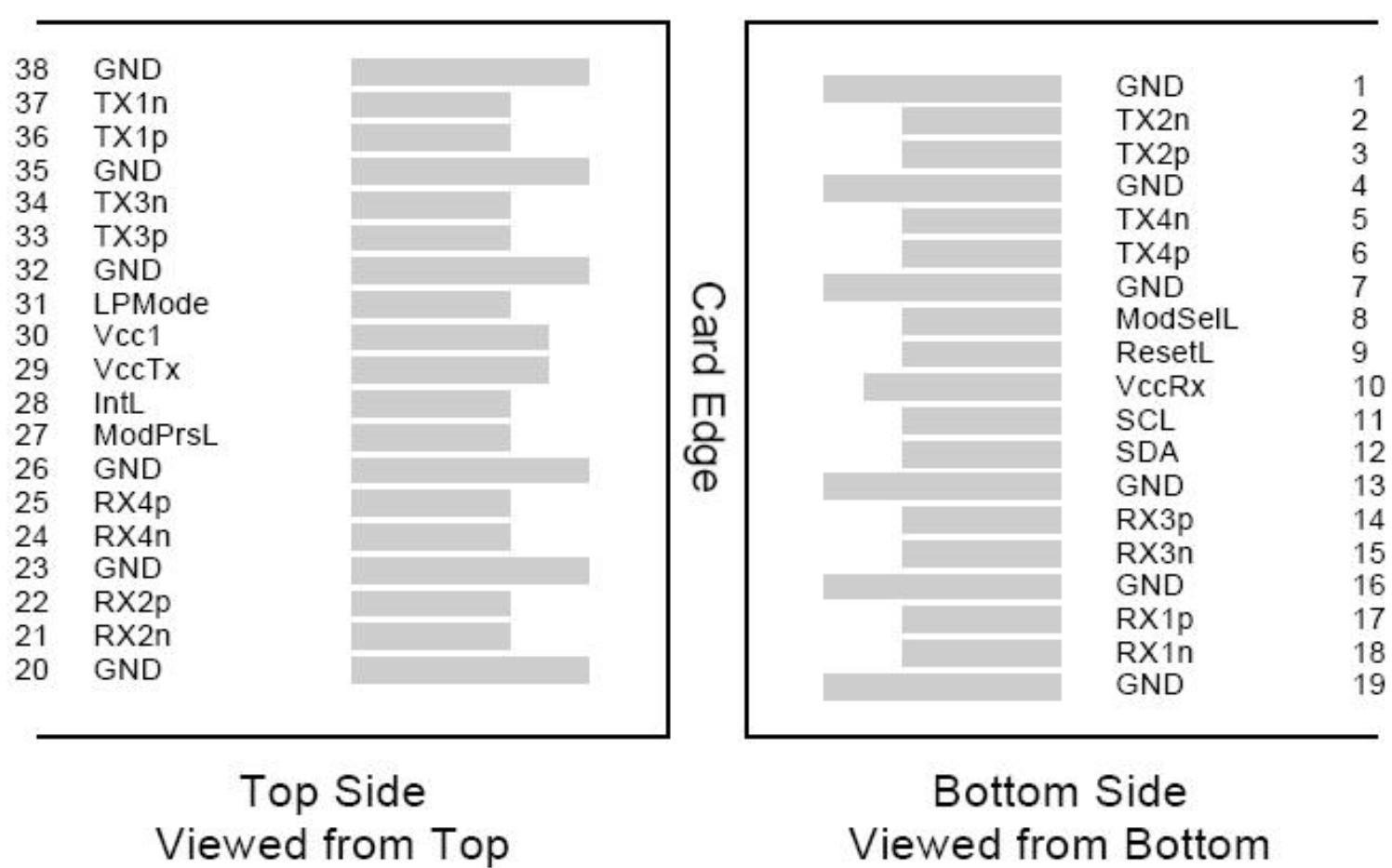
Pin Definition
PIN |
Logic |
Symbol |
Name/Description |
Notes |
1 |
|
GND |
Ground |
1 |
2 |
CML-I |
Tx2n |
Transmitter Inverted Data Input |
|
3 |
CML-I |
Tx2p |
Transmitter Non-Inverted Data output |
|
4 |
|
GND |
Ground |
1 |
5 |
CML-I |
Tx4n |
Transmitter Inverted Data Input |
|
6 |
CML-I |
Tx4p |
Transmitter Non-Inverted Data output |
|
7 |
|
GND |
Ground |
1 |
8 |
LVTLL-I |
ModSelL |
Module Select |
|
9 |
LVTLL-I |
ResetL |
Module Reset |
|
10 |
|
VccRx |
+3.3V Power Supply Receiver |
2 |
11 |
LVCMOS-I/O |
SCL |
2-Wire Serial Interface Clock |
|
12 |
LVCMOS-I/O |
SDA |
2-Wire Serial Interface Data |
|
13 |
|
GND |
Ground |
|
14 |
CML-O |
Rx3p |
Receiver Non-Inverted Data Output |
|
15 |
CML-O |
Rx3n |
Receiver Inverted Data Output |
|
16 |
|
GND |
Ground |
1 |
17 |
CML-O |
Rx1p |
Receiver Non-Inverted Data Output |
|
18 |
CML-O |
Rx1n |
Receiver Inverted Data Output |
|
19 |
|
GND |
Ground |
1 |
20 |
|
GND |
Ground |
1 |
21 |
CML-O |
Rx2n |
Receiver Inverted Data Output |
|
22 |
CML-O |
Rx2p |
Receiver Non-Inverted Data Output |
|
23 |
|
GND |
Ground |
1 |
24 |
CML-O |
Rx4n |
Receiver Inverted Data Output |
1 |
25 |
CML-O |
Rx4p |
Receiver Non-Inverted Data Output |
|
26 |
|
GND |
Ground |
1 |
27 |
LVTTL-O |
ModPrsL |
Module Present |
|
28 |
LVTTL-O |
IntL |
Interrupt |
|
29 |
|
VccTx |
+3.3 V Power Supply transmitter |
2 |
30 |
|
Vcc1 |
+3.3 V Power Supply |
2 |
31 |
LVTTL-I |
LPMode |
Low Power Mode |
|
32 |
|
GND |
Ground |
1 |
33 |
CML-I |
Tx3p |
Transmitter Non-Inverted Data Input |
|
34 |
CML-I |
Tx3n |
Transmitter Inverted Data Output |
|
35 |
|
GND |
Ground |
1 |
36 |
CML-I |
Tx1p |
Transmitter Non-Inverted Data Input |
|
37 |
CML-I |
Tx1n |
Transmitter Inverted Data Output |
|
38 |
|
GND |
Ground |
1 |
Notes:
GND is the symbol for signal and supply (power) common for the QSFP28 module. All are common within the module and all module voltages are referenced to this potential unless otherwise noted. Connect these directly to the host board signal common ground plane.
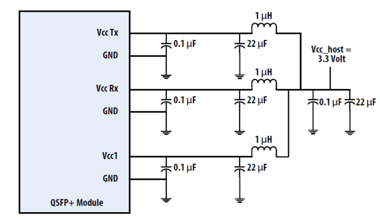
VccRx, Vcc1 and VccTx are the receiving and transmission power suppliers and shall be applied concurrently. Recommended host board power supply filtering is shown in Figure 3 below. Vcc Rx, Vcc1 and Vcc Tx may be internally connected within the module in any combination. The connector pins are each rated for a maximum current of 1000mA.
6. Absolute Maximum Ratings
Please be aware that exceeding any individual absolute maximum ratings may result in irreversible harm to this module.
Parameter |
Symbol |
Min |
Max |
Units |
Notes |
Storage Temperature |
TS |
-40 |
85 |
degC |
|
Operating Case Temperature |
TOP |
0 |
70 |
degC |
|
Power Supply Voltage |
VCC |
-0.5 |
3.6 |
V |
|
Relative Humidity (non-condensation) |
RH |
0 |
85 |
% |
|
Damage Threshold, each Lane |
THd |
5.5 |
|
dBm |
|